Fixing a legend.....

blu_fuz

Well-Known Member
Staff member
The beat up machine (video tracer #2) actually works for the most part besides the buzzing noise from it. I might be able to make that work enough for my tests.


The nice looking machine (video tracer #1) the buzzing is so loud and the signal is really distorted so this one might not be good.
 

Superduper

Moderator
Staff member
It means that you are having problems at the very beginning of the circuitry. The PCB diagram is only good for locating components and doing some tracing of the circuits. You'll have to refer and compare to the schematic diagram itself for any kind of analysis. The resistor can be bad but I think 99% that it's OK. More than likely, the resistor is isolating the bad part of circuit from good part. That's why you get good audio at one end and not so good on the other end. At this point, I recommend you do a voltage analysis of the circuit. Basically, you are going to make a copy of your schematic (if you don't want to ruin your orig). Then make spot checks of voltages based on the schematic. Then make notes along the way. If voltage check is good and consistent, then note it somehow (yellow highlight?). If voltage is not correct, then make note also (red marker?). Do this for much of the circuit. You can probably ignore the tuner section and the power amp section.
 

blu_fuz

Well-Known Member
Staff member
Oh boy.


Now would I be checking voltage power on? Power off? Sticking DMM probes where?


I want to keep going but am losing the urge to finish this. I understand this is part of the troubleshooting process, but at this rate, with kids, and many other things to do, this could take me a year or more......
 

Superduper

Moderator
Staff member
Haha, sorry bro but anyone that thinks that circuit troubleshooting is a piece of cake is sorely mistaken. It's taking you a long time because you need to stop & ask for guidance along the way but for me, I would just move right along to the next step. If you do this, then the circuit needs to be live, the BOOMBOX settings need to be consistent with settings ID'd on the schematic (otherwise voltages may not match the indicated spec). I solder/tack a eye hook (made with bent paper clip or old spent lead) onto a known good ground rail, clip black lead of tester probe to it, and all tests are done using the red probe of meter.
 

blu_fuz

Well-Known Member
Staff member
Alright, I will march on!


I will copy the schematic and get one of my clips to the ground, to my black probe lead, and probe with the red.


I put my DMM on V dc, take readings, mark as ok or not, and write down the V reading on the page where the component reading is not correct.
 

BoomboxLover48

Boomus Fidelis
Joe,
You should have a video conference with Norm. :yes:
I think you should do that... :-D
This could make things much easier. :yes:
Facetime is much easier with IPhone.
It is practically impossible to fly a Boeing 777 or Airbus 380 from the ground. :w00t:
 

blu_fuz

Well-Known Member
Staff member
I went through this schematic, clipped my black DMM lead to the negative battery terminal spring, and probed the voltage readings with my meter range set to 00.00V DC. Boombox was powered on via power cord, volume all the way down, and function switch set to line-in with no audio feeding the line-in jacks.


These are the numbers I got. There are a few numbers printed on the schematic that say "REC" above them, I'm not sure if that means I needed to have record depressed on the cassette to get a proper reading but a lot of those read "0" volts dc.


There are a few areas that the voltage readings were not close to what the schematic was telling me it should be. I don't know what the numbers mean overall, so hopefully someone can see maybe a problem area and shed some light. Thanks guys.

There is a PDF below that is much more clear. Open that up and rotate the view 90* counterclockwise.


Scan0001.jpg
Scan0002.jpg
View attachment Scan.pdf
 

Superduper

Moderator
Staff member
Superduper said:
................ The PCB diagram is only good for locating components and doing some tracing of the circuits. You'll have to refer and compare to the schematic diagram itself for any kind of analysis. ............................
Need the schematic Joe.
 

Ken

Member (SA)
You're doing fine, Joe. :-D

In this case, considering the learning curve you are up against, slow & steady will win the race. A wiser man than I told me that once. All I know is that you've got top-notch talent in your corner, Joe, and it's got faith in you. So you can have some of that in yourself anytime you feel like it. Heck, I have a current project that I have applied some of the techniques from this thread to.

Take your time. Play with the kids. Don't forget to enjoy your other boxes. You're in this for the long haul. ;-)
 

blu_fuz

Well-Known Member
Staff member
I have the schematic, but I can't flip my 5350 PCB around or move it from its position to verify all the bits on the schematic trying to check voltages. This is a tough box to need powered on and almost 100% dismantled to check things like this (like you said already it would be). It was easier and really the only way I could do it was from the diagram for now.


I have not gone through it like I did with the diagram, but I do have readings written on my diagram that can be crossed with the schematic.
 

Superduper

Moderator
Staff member
It may not be obvious at first, but after I explain, you'll see.

The reason I mentioned to mark up the SCHEMATIC and not use the PCB diagram, is because if there is a voltage discrepency, I can immediately see at a glance all the appurtenant adjacent components. For example, if pin 10 of an IC is supposed to read "0" volts and you are getting 8.2V, and I can see on the schem that pin 10 goes to ground, it tells me immediately that you have a break in the connection from pin 10 to ground. See what I mean? However, on the PCB diagram, we can see an actual illustration of the IC and pin 10, which is real pretty and completely accurate to your actual physical board. But I can't tell where pin 10 is connected to, as the trace might flip across the board several times, might terminate at a location 8 inches away and still doesn't tell me what the next pad is connected to relative to the rest of the circuit. On the other hand, the PCB diagram is great for locating say...... C307 which without the PCB diagram, means trying to handle and scan the PCB. Even if you know C307 is connected to R307, you don't know if those two components are actually 6" apart when on the schem, it looks like they are right next to each other. Worse, if the actual PCB has no printed legends, it's almost impossible to determine which component is what without a PCB diagram. So it has it's place and purpose, but for what we need to do right now, you need to work with the schematic. Once you've marked it up you can do almost all your diagnostics on the desk rather than on the bench. Make sense now?

Any frustration is completely understandable. You are a fast learner and fearless. That will get you far. Many would have bailed by now, which is the safe route. But they won't learn what you will. As I said, and as you already know, this is a challenging boombox to work on due to the nature of how the PCB is mounted in the cabinet, and difficulty in getting below board access while powered up. You can do this one, you can do most others.
 

blu_fuz

Well-Known Member
Staff member
Thanks for the push guys and the compliments Norm. I do love to learn new things, so this is right up my alley. Usually only need to be told once (or twice) to get full understanding of a new task.


I totally understand exactly what you are saying now on why I should mark on the schematic.


I will get my readings written onto the schematic and scan it again so it can bee seen in one shot.


:cool:
 

oldskool69

Moderator
Staff member
I am going to make this a sticky. I will also find out if we can move this to the section with the other permanent brand occupants in the tech section. :-D
 

blu_fuz

Well-Known Member
Staff member
Since the schematic is a visual of the circuits and the diagram is a visual of the board, I'm glad I started with writing on the board diagram page because they lay out the test points, values, and are really easy to follow for someone new to this like me. Now when I look at the schematic it makes more sense to me what I am looking at. The values I wrote on the board diagram page make it easy to find the correct spots on the schematic.


Life got hectic after I posted last and I didn't get a chance to swap the written values over to the schematic. Hopefully tonight and I will post them up.


I'm starting to understand why these original service manuals are so important. Even the PDF versions of service manuals are good for something, but almost impossible to follow unless you print them off and they NEED to be in full color for a newbe like me. I can't thank you guys enough for the original manual I was able to copy in full color and full size (skippy), and the all tips from Norm and everyone else in here.
 

blu_fuz

Well-Known Member
Staff member
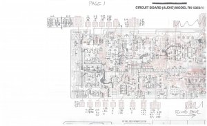
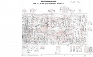
Here is the PDF of the schematic diagram WITH the voltage readings that seemed either too high or too low. There isn't a lot of room to write the values on that page by the components, so I'm sorry if it is too tight or small.

I noted on the side of each page the approx. location of the part in question with an arrow pointing towards the direction it is in.

Any part with a check mark by it, the voltage readings were either exact or close to the value shown in red and didn't raise any flag to note them.


I hope this is good.
 

Attachments

  • Scan0002.pdf
    1.2 MB · Views: 27

Superduper

Moderator
Staff member
Ok, my eyes are weary now from doing the periscope thing with the diagram. Here are some things I would do:

Check: Base of Q407 is connected to R458 (100k), which goes to S2-12. This looks like a power rail. You must check for continuity. In other words, it appears 1 leg of R458 connects to 1 leg (opposite from Q407) of R468. Confirm no breaks.

Note: All those little lines that ends in arrow.... usually, they are jumpers and for ease of schematic draw, the other end terminates in an orientation pointed at by the direction of the arrow. You will need to confirm these.

IC402: Can't read the correct voltage. Is that supposed to be 3V but reading 8.49? What is the IC part no?

IC403: Check R420 (4.7k)

Q401, can't read the voltages

Q406, you are reading higher than spec'd voltage because you are feeding circuits from mains (unregulated) instead of +15v as likely specified in schematic setup notes. Usually, we power up the boombox using lab power supplies. Many voltages will be off a bit, especially those parts of the circuits that are unregulated, when you use power that is outside of the prescribed amount for testing. All board voltages are likely to be intended for testing by powering up via a +15v power supply.

Q411: You are getting 9 volts because schematic shows S15 & S3-3 is supposed to be in the closed position for test. Not sure if all your settings are correct. Confirm those switches are thrown.

Q410: I can't read the voltage. But the collector appears is connected to (+) rail when S13/12 is closed. Not sure what those switches are... motor play switch? If those are not closed, you won't see voltage at Q410 collector. Also several lines go through connector CP203. Even if those switches are closed, if CP203 has bad connections, the circuit will be broken. Anyhow, you can investigate but this discrepency doesn't interest me that much right now since I am presuming the hum occurs regardless of setting so this probably isn't related since the lack of voltage depends on the switch position and your issue is not setting specific.

Q408. Eh... I dunno know that those readings interest me that much. IF the readings I am interpreting is what the actual are. They don't come in clear for me.

IC102/202: Are power amplifiers. If you wanna know if they are OK, just inject an audio signal into pin 6 using an audio signal generator, or just use the center pin of a line-out jack, or an MP3 device. If you get good loud audio, then move on.

Not sure if I missed anything. Oh, I'm not gonna comment on any voltage discrepency on those transistors with a <v> readings. That's because I am presuming those readings are signficant under certain <> settings which might be record, etc. There is a reason those readings are identified within brackets when everything else is without. That being the case, I presume the readings you are getting don't apply to the current settings.

Also check R469 and make sure it's reading correct, AND the other leg is grounded properly (check ground leg resistance to a known good ground).

Well, let's start with those. Especially look at the discrepency issue at Q407.
 

k2j

Member (SA)
This is awsome. Loved the video Joe, my suggestion get it off that floor it looks like a static nightmare!! Also, agree with norm, get yourself a good bench power supply and feed it a good steady supply of DC.

Keep up the good work guys this is inspirational!
 

blu_fuz

Well-Known Member
Staff member
Superduper said:
Ok, my eyes are weary now from doing the periscope thing with the diagram. Here are some things I would do:

Check: Base of Q407 is connected to R458 (100k), which goes to S2-12. This looks like a power rail. You must check for continuity. In other words, it appears 1 leg of R458 connects to 1 leg (opposite from Q407) of R468. Confirm no breaks.

Note: All those little lines that ends in arrow.... usually, they are jumpers and for ease of schematic draw, the other end terminates in an orientation pointed at by the direction of the arrow. You will need to confirm these.
I confirm what you said, B leg of Q407 is connected to R458 and I can confirm that the circuit ends up at S2-12. If you follow Q407 B leg through the vias, showing red line on diagram (printed trace), to printed resistor R458, then to another vias. From the last vias it splits to 3 spots:
- to jumper, traces to #1 on CP203
- traces over to R468 then down to #1 pin by S2-12
- traces to jumper, then off of page #1

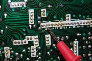
I just realized after I typed all this and traced the board diagram again, that I probed the wrong pin at S2-12! I will have to go back and check pin #1, not pin #2 like shown below. Sorry about that, grrrr.


Q407 shown below:
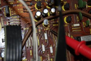
DSC_0319.JPG

The R458 is a printed resistor (shown as black square) shown below:
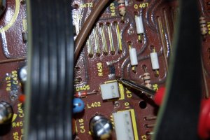
DSC_0320.JPG


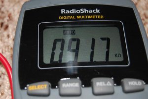
Checking continuity from the B leg of Q407 to pin #2 @ S2-12 nets me 0 continuity and 91.7 k-ohm resistance:
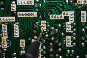
DSC_0321.JPG
DSC_0322.JPG
DSC_0323.JPG


IC402: Can't read the correct voltage. Is that supposed to be 3V but reading 8.49? What is the IC part no?

IC402 part number from the book is RVIBA328. The IC itself has numbers:
BA328
208 351

That IC is also located in the area that got hit the worst with the battery acid.
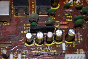
DSC_0327.JPG


You are correct, the reading at pin #3 should be 3V but is reading 8.49V.

IC402
1) 1.4v reading = 0.76v
2) 0.9v reading = 0.16v
3) 3v reading = 8.49v
4) 7.7v reading = 8.5v
5) 0v reading = 0.01v
6) 3.1v reading = 4.08v
7) 0.9v reading = 0.91v
8) 1.4v reading = 1.47v


IC403: Check R420 (4.7k)

^ok, will check it off


Q401, can't read the voltages

Q401
C) 0v reading = 0v
B) 0.8v reading = 0v
E) 0v reading = 0v


Q406, you are reading higher than spec'd voltage because you are feeding circuits from mains (unregulated) instead of +15v as likely specified in schematic setup notes. Usually, we power up the boombox using lab power supplies. Many voltages will be off a bit, especially those parts of the circuits that are unregulated, when you use power that is outside of the prescribed amount for testing. All board voltages are likely to be intended for testing by powering up via a +15v power supply.

^ok, I did notice that there was a consistant higher amount of voltage readings on a few components. Seemed like these were not areas I should be too worried about and that makes sense why now that you explained using a power supply.


Q411: You are getting 9 volts because schematic shows S15 & S3-3 is supposed to be in the closed position for test. Not sure if all your settings are correct. Confirm those switches are thrown.

^ I noticed that the schematic notes tell me what positions the switches need to be in for testing. I didn't see that list of "notes" until after I was all finished and looking back over the paperwork. Sorry about that. I will still verify the switch positions and check again and will post any fishy readings.


Q410: I can't read the voltage. But the collector appears is connected to (+) rail when S13/12 is closed. Not sure what those switches are... motor play switch? If those are not closed, you won't see voltage at Q410 collector. Also several lines go through connector CP203. Even if those switches are closed, if CP203 has bad connections, the circuit will be broken. Anyhow, you can investigate but this discrepency doesn't interest me that much right now since I am presuming the hum occurs regardless of setting so this probably isn't related since the lack of voltage depends on the switch position and your issue is not setting specific.

Q410
C) 15v reading = 0v
B) 0v reading = 0v
E) 0v reading = 0v

I'm not sure what those switches are either. You are correct, the hum/buzzing in the system occurs regardless of switch setting.


Q408. Eh... I dunno know that those readings interest me that much. IF the readings I am interpreting is what the actual are. They don't come in clear for me.

Q408
C) 8.4v reading = 0.65v
B) 7.6v reading = 9.0v
E) 8.4v reading = 9.0v


IC102/202: Are power amplifiers. If you wanna know if they are OK, just inject an audio signal into pin 6 using an audio signal generator, or just use the center pin of a line-out jack, or an MP3 device. If you get good loud audio, then move on.

^ ok, I'll give that a whirl :cool:. I didn't have a chance to test your method.

IC102
1) 0v reading = 0v
2) 7.5v reading = 9.36v
3) 14.7v reading = 8.66v
4) 14.8v reading = 18.86v
5) 1.3v reading = 1.23v
6) 0v reading = 0.03v
7) 0v reading = 0v
8) 1.3v reading = 1.21v
9) 14.7v reading = 1.21v
10) 15v reading = 18.94v
11) 7.4v reading = 9.43v
12) 0v reading = 0v

IC202
1) 0v reading = 0v
2) 7.5v reading = 9.25v
3) 14.7v reading = 8.66v
4) 14.8v reading = 18.86v
5) 1.3v reading = 1.23v
6) 0v reading = 0.03v
7) 0v reading = 0v
8) 1.3v reading = 1.21v
9) 14.7v reading = 1.21v
10) 15v reading = 18.94v
11) 7.4v reading = 9.53v
12) 0v reading = 0v


Not sure if I missed anything. Oh, I'm not gonna comment on any voltage discrepency on those transistors with a <v> readings. That's because I am presuming those readings are signficant under certain <> settings which might be record, etc. There is a reason those readings are identified within brackets when everything else is without. That being the case, I presume the readings you are getting don't apply to the current settings.

^ correct, those transistors have "REC" marked above the voltage specs and I did not have the boombox in any cassette mode/function at all during the tests.


Also check R469 and make sure it's reading correct, AND the other leg is grounded properly (check ground leg resistance to a known good ground). Well, let's start with those. Especially look at the discrepency issue at Q407.


R469 is another printed resistor that snakes under R459:
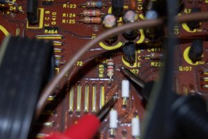
DSC_0324.JPG


I checked R469 for continuity and resistance from vias to vias across the printed resistor. Results 0 continuity and resistance is 1.916 k-ohm. I checked R469 for continuity and resistance from ground to lower vias shown in the picture. Results showing continuity good and 0 resistance.
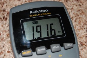
DSC_0325.JPG


I also checked R459 which is a regular resistor (not printed), because I wasn't sure if you really wanted me to check R459 and not R469 so I checked this one anyway since I was in there. Results from ground to lower lead shown in picture, results continuity good and 0 resistance.